Semiconductor High Performance Ceramics Market Projected at 3674 Million USD by 2026 – Shifting Competitive Landscape


Semiconductor High-Performance Ceramics Market Summary
According to the new market research report “Global Semiconductor High-Performance Ceramics Market Report 2026-2032”, published by QYResearch, the global Semiconductor High-Performance Ceramics market size is projected to reach USD 5.6 billion by 2032, at a CAGR of 7.3% during the forecast period.
Figure. Global Semiconductor High-Performance Ceramics Market Size (US$ Million), 2020-2031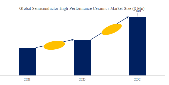
Above data is based on report from QYResearch Semiconductor Research Center: Global Semiconductor High-Performance Ceramics Market Report 2025-2031 (published in 2025). If you need the latest data, plaese contact QYResearch.
Engineered technical ceramics are used in the semiconductor industry because of their excellent material properties.
This report studies the structural ceramic components used in semiconductor wafer processing, and semiconductor fabrication (front end). Key ceramic components for crystal silicon pulling, deposition (CVD, PVD, ALD, Etch, High Temp Processing, Ion Implant, Lithography & Wafer Inspection, Diffusion & LPCVD Processing, CMP, and Wafer Handling, etc.
Semiconductor High-Performance (structural) ceramics have become a critical enabling material set rather than a “generic parts category,” because they sit directly in the most yield-sensitive and plasma-intensive parts of the toolset—most notably electrostatic chucks (ESCs), ceramic heaters, wafer/vacuum chucks, chamber rings/liners, and other precision chamber components. NGK explicitly positions its high-performance ceramics business around heaters and electrostatic chucks for semiconductor manufacturing, and notes it also manufactures chamber components using materials such as aluminum nitride and aluminum oxide for a range of applications. Kyocera describes ESCs as used for wafer mounting, flatness correction and wafer cooling during semiconductor manufacturing, highlighting why ceramics’ dielectric/thermal/mechanical properties translate directly into process stability. CoorsTek’s semiconductor portfolio illustrates how ceramics map to actual process hardware, e.g., focus/edge rings designed to improve etch uniformity and commonly used together with an electrostatic chuck in plasma etch tools. The revenue distribution you provided (large first tier led by NGK, Kyocera, Niterra, CoorsTek, Ferrotec, TOTO, etc., plus a long tail of specialized and emerging suppliers) matches the sector’s reality: high customer-qualification barriers, tight purity/trace-metal control, and precision manufacturing capability tend to concentrate share in established leaders, while newer entrants often start from narrower product niches or regional substitution programs.
Figure. Global Semiconductor High-Performance Ceramics Top 40 Players Ranking and Market Share (Ranking is based on the revenue of 2024, continually updated)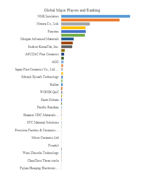
Above data is based on report from QYResearch Semiconductor Research Center: Global Semiconductor High-Performance Ceramics Market Report 2025-2031 (published in 2025). If you need the latest data, plaese contact QYResearch.
The global market is dominated by few players from US, Japan, South Korea, Europe and South Korea, key players include NGK Insulators, Kyocera, Coorstek, Niterra Co., Ltd, Ferrotec, TOTO Advanced Ceramics, Morgan Advanced Materials, MiCo Ceramics Co., Ltd. and Suzhou KemaTek, Inc., etc. Global top seven players hold a share over 80%. And in next few years, the giants like NGK Insulators, Coorstek, Kyocera, TOTO Advanced Ceramics, Morgan Advanced Materials and Ferrotec, will play more roles in next six years, these giants strengthen their place through expansion and acquisitions.
Looking forward, the strongest growth tailwinds come from “process harshness” and “tool intensity,” not just wafer starts. As device scaling shifts more pattern transfer burden to plasma etch/clean, ceramics must withstand increasingly corrosive halogen/fluorine-based plasmas used in etching and chamber cleaning. This is driving a clear materials trend toward higher plasma-erosion-resistance ceramics (beyond conventional alumina), where yttria-based systems are widely studied and recognized for superior erosion resistance in fluorine plasmas; recent work specifically discusses Y₂O₃ ceramics as erosion-resistant materials in CF₄ etching plasma, and related studies compare protective yttrium-based compositions/coatings for fluorine-plasma exposure. In parallel, tighter overlay/CD budgets and higher power densities raise demand for thermal-management ceramics (e.g., AlN-based heaters/ESC platforms) and tighter dimensional stability, because wafer temperature uniformity and chuck performance increasingly gate yield and throughput. On the commercial side, demand is trending more “consumable-like”: ceramics in etch/deposition chambers and wafer handling systems are replaced or refurbished on cadence to control particles/contamination and maintain tool uptime, so growth is supported by both installed-base expansion and more frequent parts turnover at advanced processes. Suppliers such as Morgan explicitly frame semiconductor ceramic components around helping fabs optimize processes, increase yield, and reduce total cost of ownership, which is why ceramics content typically rises as customers push for higher utilization and tighter defect budgets.
Junping Yang is a technology & market senior analyst specializing in semiconductor supply chain, like IC design (Fabless/IDM), wafer fabrication (Pure play foundries/IDM), IC Packaging/Testing (IDM/OSAT), semiconductor materials (Wafer Fab Materials and Packaging Materials), and semiconductor equipment and parts. Yang has 11 years’ experience in semiconductor and focuses semiconductor equipment/parts, materials (silicon wafer, photoresist, CMP, silicon electrodes and rings), ICs, discrete devices, sensors/MEMS, RF, package & testing, etc. Typical studies include ICs, power semiconductor (IGBT, SiC, diode, MOSFET, modules and discrete), compound semiconductor (SiC, GaN, etc.), RF, optoelectronics, ceramic substrates (HTCC, LTCC, DBC, AMB, DPC, DBA), equipment & parts (wafer transfer robot, EFEM/Sorter, heaters, chiller, etc.), Lithography Systems, semiconductor refurbished/used equipment and parts, semiconductor chamber cleaning/coating, semiconductor equipment parts (ceramics, metal, plastic), Lasers, Electronic Ceramics, etc. He is engaged in the development of technology and market reports and is also involved in custom projects.
About QYResearch
QYResearch founded in California, USA in 2007. It is a leading global market research and consulting company. With over 17 years’ experience and professional research team in various cities over the world QY Research focuses on management consulting, database and seminar services, IPO consulting, industry chain research and customized research to help our clients in providing non-linear revenue model and make them successful. We are globally recognized for our expansive portfolio of services, good corporate citizenship, and our strong commitment to sustainability. Up to now, we have cooperated with more than 60,000 clients across five continents. Let’s work closely with you and build a bold and better future.
QYResearch is a world-renowned large-scale consulting company. The industry covers various high-tech industry chain market segments, spanning the semiconductor industry chain (semiconductor equipment and parts, semiconductor materials, ICs, Foundry, packaging and testing, discrete devices, sensors, optoelectronic devices), photovoltaic industry chain (equipment, cells, modules, auxiliary material brackets, inverters, power station terminals), new energy automobile industry chain (batteries and materials, auto parts, batteries, motors, electronic control, automotive semiconductors, etc.), communication industry chain (communication system equipment, terminal equipment, electronic components, RF front-end, optical modules, 4G/5G/6G, broadband, IoT, digital economy, AI), advanced materials industry Chain (metal materials, polymer materials, ceramic materials, nano materials, etc.), machinery manufacturing industry chain (CNC machine tools, construction machinery, electrical machinery, 3C automation, industrial robots, lasers, industrial control, drones), food, beverages and pharmaceuticals, medical equipment, agriculture, etc.

Global Semiconductor High Performance Ceramics Market Insights - Industry Share, Sales Projections, and Demand Outlook 2026-2032

Published Date: 2026-03-06

Pages: 158

Report ld: 6019345
Price:USD 3200.00
(Single User License)
Global Semiconductor High Performance Ceramics Market Outlook, In‑Depth Analysis & Forecast to 2032
Published Date: 2026-01-28
Pages: 220
Report ld: 5583706
Price:USD 4900.00
(Single User License)
Global Semiconductor High Performance Ceramics Sales Market Report, Competitive Analysis and Regional Opportunities 2026-2032
Published Date: 2026-01-28
Pages: 136
Report ld: 5569851
Price:USD 4250.00
(Single User License)
Global Semiconductor High Performance Ceramics Market Research Report 2026
Published Date: 2026-01-28
Pages: 183
Report ld: 5519491
Price:USD 2900.00
(Single User License)
Semiconductor High Performance Ceramics - Global Market Share and Ranking, Overall Sales and Demand Forecast 2026-2032
Published Date: 2026-01-28
Pages: 198
Report ld: 5509745
Price:USD 3950.00
(Single User License)
Semiconductor High Performance Ceramics - Global Market Share and Ranking, Overall Sales and Demand Forecast 2025-2031
Published Date: 2025-10-10
Pages: 190
Report ld: 3690746
Price:USD 3950.00
(Single User License)


Competition
Key players, new entrants,acquisitions, mergers and expansions,development trends and challenges.

Industry Analysis
Rawmaterial, application, product type, demand,supply,downstream, supply chain etc.

Market Size
Capacity, production, sales, revenue, price, cost etc.

Customized Information
We can offer customized survey and information to meet ourclient's need.
