EDS/EDX detector Market Research:representing a CAGR of approximately 8% from 2025 to 2032


EDX detectors, also commonly known as EDS detectors, Energy Dispersive X-ray detectors, or energy-dispersive X-ray detectors, are core detection components in energy-dispersive X-ray spectroscopy analysis systems. Their main function is to receive the characteristic X-rays emitted after a sample is excited by an electron beam or X-rays, and convert X-ray signals of different energies into identifiable and quantifiable electrical signals, thereby enabling qualitative and quantitative elemental analysis and imaging of elemental surface distribution. This product is typically used in conjunction with scanning electron microscopes (SEM), transmission electron microscopes (TEM/STEM), electron probe microanalysis, and X-ray fluorescence analyzers (XRF/EDXRF), and is an important module for micro-area compositional analysis, failure analysis, quality control, and scientific characterization of materials. In a narrow industry definition, EDX detectors primarily include SDD, Si(Li), and Si-PIN detector hardware and their directly related electronic modules, and should not include the entire SEM, TEM, and XRF mainframes, sample preparation equipment, software services, and consumables. Oxford Instruments defines EDS/EDX as a technology for elemental and compositional analysis based on X-ray information generated after electron irradiation of samples; JEOL also points out that EDS achieves elemental analysis by detecting characteristic X-rays emitted from samples.
The global EDS/EDX detector market belongs to a high-tech segment within scientific instruments and materials characterization equipment. While individual market sizes are relatively small, it boasts high technological barriers, strong customer loyalty, and significant complementary value. Based on sales revenue, the global EDS/EDX detector market was approximately $85.4 million in 2025 and is projected to reach approximately $147 million by 2032, representing a CAGR of approximately 8% from 2025 to 2032. This growth rate is faster than that of most traditional analytical instrument components, reflecting structural demand driven by upgrades in semiconductors, advanced materials, lithium batteries, new energy, aerospace, electronics manufacturing, and research platforms. The current market has shifted from a phase dominated by traditional Si(Li) detectors to an upgrade phase centered on SDD (Silicon Drift Detector). The focus of demand has shifted from "elemental analysis capability" to "high count rate, high energy resolution, large-area detection, low-energy element detection, fast mapping, low-current and low-voltage analysis, and automated data processing." Thermo Fisher technical data indicates that SDD has become the mainstream advanced solution for high-resolution, high-count-rate X-ray spectroscopy analysis; manufacturers such as Bruker and Oxford Instruments are also continuously upgrading their products to focus on larger detection areas, higher throughput, and stronger low-energy peak resolution capabilities.
From a product segmentation perspective, EDX detectors can be categorized by detector technology, application equipment, detection area, window structure, cooling method, and system integration method. In terms of technology, SDD (Self-Driving Detector) is currently the mainstream and fastest-growing approach, offering advantages such as no need for liquid nitrogen cooling, high count rate, good stability, and suitability for rapid spectral acquisition and elemental mapping. Si(Li) detectors are an earlier solution, still used in some existing equipment and specific laboratory scenarios, but new demand is continuously being replaced by SDD. Si-PIN detectors are more commonly used in cost-sensitive EDXRF or portable/entry-level analysis systems. In terms of detector area, 30mm², 60mm², 80mm², 100mm², and multi-probe combinations correspond to different sensitivity, space constraints, and analytical efficiency requirements. Large-area, ring-shaped, and windowed/windowless detectors are more suitable for low-current, low-voltage, nanomaterial, and high-throughput surface distribution analysis. Bruker's XFlash series emphasizes high throughput and high geometric collection efficiency, Thermo Fisher's UltraDry detectors offer an effective area of up to 100 mm² and support a unified software platform for EDS, WDS, and EBSD, while Hitachi's Vortex-ME7 seven-element SDD system achieves an effective area of 210-350 mm². This indicates that the industry is upgrading towards "large area, high throughput, multi-element arrays, and platform integration."
The application scenarios for EDX detectors are mainly concentrated in materials science, semiconductors and electronics, industrial quality control, geology and minerals, metallurgy, lithium batteries and new energy, environmental compliance, life sciences, and scientific research and education. In materials science, EDX/EDXRF systems are used for micro-area elemental analysis of phase composition, inclusions, coatings, composites, and nanomaterials. In semiconductor and electronics manufacturing, they are used for failure analysis, contaminant localization, thin-film/interconnect structure detection, and packaging material analysis. In metallurgy, they are used for inclusion analysis, alloy composition confirmation, and fracture analysis. In lithium-ion batteries, new energy, and catalytic materials, they focus on electrode materials, particle distribution, elemental migration, and interface changes. EDX/EDXRF systems have wide applications in RoHS/ELV, consumer product environmental screening, food packaging, ore, soil, and liquid sample analysis. Shimadzu's EDX-8100 can be used for elemental analysis of various samples, covering the elemental range from C to U, while the EDX-LE series is designed for RoHS/ELV restricted element screening, demonstrating the application value of EDX/EDXRF in industrial compliance and rapid detection. Future faster-growing applications are expected in semiconductor failure analysis, advanced materials R&D, lithium-ion battery materials, nanomaterials, precision manufacturing quality control, and university research platform upgrades, while demand for traditional mineral, metallurgical, and general laboratory analysis remains relatively stable.
The global competitive landscape for EDX detectors is characterized by a few leading international manufacturers dominating the high-end market, system integration capabilities determining customer loyalty, and companies specializing in detector modules participating in upstream supply. Companies like Oxford Instruments, Bruker, AMETEK EDAX, Thermo Fisher Scientific, and JEOL possess strong competitiveness in SEM/TEM/EDXRF components, detector hardware, spectrometer systems, acquisition electronics, and analysis software. Companies such as KETEK, PNDetector, and Amptek participate more in the industry chain through detector modules, SDD chips, or X-ray detection components. Competition in the high-end market extends beyond detector hardware parameters; it also includes mechanical compatibility with microscope platforms, vacuum interfaces, geometric collection angles, electronic noise control, peak overlap resolution, low-energy element detection, real-time element mapping, quantitative algorithms, software ecosystems, and after-sales service capabilities. Bruker XFlash 7 emphasizes element mapping speed and geometric collection efficiency, while Oxford Instruments Ultim Max Infinity emphasizes low-energy peak overlap resolution and complex analysis capabilities, indicating that leading manufacturers are shifting from competition based solely on hardware specifications to systemic competition encompassing "detector + electronics + algorithm + software workflow." For new entrants, the key challenges lie in high-purity silicon detector fabrication, low-noise front-end electronics, vacuum and thermal management, quantitative algorithms, long-term stability verification, and ecosystem integration with mainstream SEM/TEM manufacturers.
Regionally, North America, Europe, and Japan are key hubs for EDX detector technology, brands, and high-end demand, primarily benefiting from a mature electron microscopy industry base, advanced materials research, semiconductor manufacturing, life science platforms, and industrial testing systems. The US and Europe are strong in detector modules, analytical software, scientific instrument brands, and high-end laboratory demand, while Japan has advantages in electron microscope mainframes, industrial testing, and precision manufacturing applications. China and the broader Asia-Pacific region represent one of the markets with the highest growth potential, driven by demand from semiconductor localization, expansion of materials R&D platforms, upgrades to university research instruments, new energy materials, automotive electronics, third-party testing, and quality control upgrades in manufacturing. In the short term, the Chinese market will remain dominated by imported brands and international system solutions, but with the advancement of domestic substitution for SEM, TEM, XRF, and scientific instruments, EDX detectors and their upstream SDD chips, low-noise electronics, algorithm software, and overall system compatibility will become key areas for localization efforts. Overall, mature markets will continue to be driven by high-end demand and technical standards, while the Asia-Pacific market, especially China, will contribute to new installations and domestic substitution. The global market will present a pattern of "leading high-end technologies in Europe, the US, and Japan, faster demand growth in China and the Asia-Pacific region, and increasing importance of system integration and local services."
Figure00001. EDX Detectors Market Structure
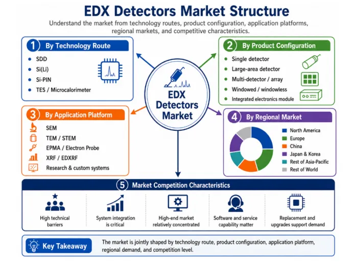
Figure from QYResearch: Global EDX Detectors Market Report 2026-2032.
From a market structure perspective, EDX detectors are not ordinary sensors independent of the main instrument unit, but rather a high-end scientific instrument core component market formed by technological routes, configuration specifications, application equipment, regional needs, and system integration capabilities. By technological route, SDD (Silicon Drift Detector) has become the mainstream growth direction, mainly benefiting from advantages such as high count rate, high stability, low noise, and no need for liquid nitrogen cooling; Si(Li) detectors are more prevalent in some existing equipment and specific laboratory scenarios, while Si-PIN detectors are geared towards cost-sensitive or entry-level analytical systems. By product form and configuration, the market is further segmented into single-probe, large-area detectors, multi-probe/array, window/windowless detectors, and integrated electronics modules. Different configurations correspond to different spatial resolutions, collection angles, low-energy element detection capabilities, and high-speed mapping requirements. JEOL's description of EDS indicates that EDS achieves elemental analysis by detecting the characteristic X-rays emitted by a sample under electron beam irradiation; Oxford Instruments also positions EDS/EDX as a technology for elemental and compositional analysis based on X-ray information, which determines that detector performance, geometric collection efficiency, and spectral processing capabilities are the core variables in the market structure. From the perspective of application equipment and competitive landscape, EDX detectors mainly form supporting demands around SEM, TEM/STEM, EPMA/electron probe microanalysis, XRF/EDXRF, and other micro-area analysis platforms. Their downstream growth is highly correlated with semiconductors, advanced materials, lithium-ion batteries, metallurgy, geology and minerals, quality inspection, and the construction of scientific research platforms. The high-end market has a relatively high concentration, and competition is not just about individual detector hardware parameters, but rather a comprehensive competition encompassing "detector chips + low-noise electronics + vacuum/mechanical adaptation + analysis software + element mapping algorithms + host platform ecosystem." Bruker's XFlash series covers different detector sizes, shapes, and window materials, emphasizing maximizing the X-ray collection angle; Oxford Instruments' EDS system targets micro-nano scale elemental analysis in SEM, TEM, and FIB, indicating that the industry is shifting from selling single detectors to platform-based, software-based, and application-scenario-based solutions. At the regional level, North America, Europe, and Japan still have a strong technology and customer base in high-end instruments, semiconductors, and advanced materials applications, while China and other Asia-Pacific markets are driven by the expansion of scientific research platforms, the localization of semiconductor production, the research and development of new materials, and the upgrading of industrial testing, resulting in greater elasticity of new demand.
Figure00002. EDX Detectors Industry Chain
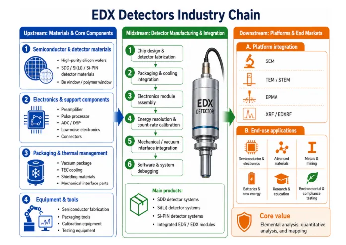
Figure from QYResearch: Global EDX Detectors Market Report 2026-2032.
From the upstream perspective of the industry chain, the core investment in EDX detectors is not ordinary electronic components, but a high-barrier supply system comprised of semiconductor detection materials, low-noise electronics, vacuum packaging, thermal management components, and precision testing equipment. The semiconductor and detection materials segment mainly includes high-purity silicon wafers, SDD/Si(Li)/Si-PIN detector chip materials, and window materials such as Be windows or polymer windows; the electronics and supporting device segment includes preamplifiers, pulse processors, ADCs/DSPs, low-noise circuits, and connectors; the packaging and thermal management segment involves vacuum packaging, TEC cooling/refrigeration components, shielding materials, and mechanical interface components. Since the working principle of EDX/EDS is to receive the characteristic X-rays generated after the sample is excited by an electron beam and perform elemental composition analysis, the detector's energy resolution, count rate, low-energy element response, and noise control directly determine the performance ceiling of the entire analysis system. Oxford Instruments defines EDS/EDX as a technology for elemental and compositional analysis based on X-ray information generated by electron irradiation of samples. Thermo Fisher also points out that SDD is an advanced solution for high-resolution, high-count-rate X-ray spectroscopy analysis, with significantly improved performance compared to traditional Si(Li) detectors. This indicates that upstream detector chips, low-noise electronics, and thermal management capabilities are the key foundations of the EDX detector industry chain.
From a midstream and downstream perspective, the value of EDX detector manufacturing is mainly concentrated in system integration stages such as chip design and material selection, detector chip manufacturing, packaging and cooling integration, electronics module assembly, energy resolution and count rate calibration, host platform adaptation, and software integration. Midstream companies not only need to produce individual detector hardware but also solve problems related to mechanical interfaces, vacuum environments, geometric collection angles, signal processing, spectral algorithms, and software workflow adaptation with host platforms such as SEM, TEM/STEM, EPMA, and XRF/EDXRF. Downstream applications cover semiconductors and electronics, advanced materials, metallurgy, lithium batteries and new energy, geology and minerals, scientific research and education, industrial quality control, and environmental and compliance testing. Its core value lies in achieving elemental analysis, quantitative analysis, elemental surface distribution mapping, and high-sensitivity detection. Bruker's EDS detector product line emphasizes its applicability to platforms such as SEM, FIB-SEM, and EPMA, and supports rapid elemental mapping. Oxford Instruments also positions its EDS system for micro- and nano-scale elemental and chemical analysis in SEM, TEM, or FIB. Therefore, the EDS detector industry chain is upgrading from a single hardware supply chain to a comprehensive solution system of "detector chip + electronics module + host adapter + analysis software + application services".
Figure00003. Working Principles of EDX Detectorss Based on Different Technical Approaches
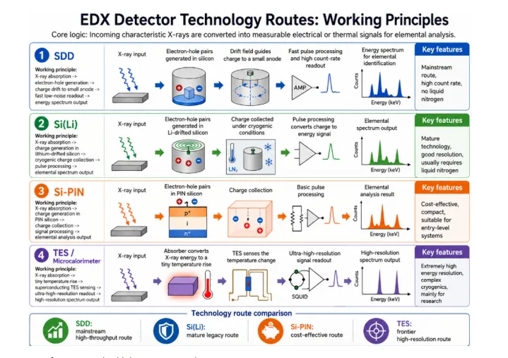
Figure from QYResearch: Global EDX Detectors Market Report 2026-2032.
From a technical perspective, the core working logic of EDX detectors is as follows: a sample releases characteristic X-rays under electron beam or X-ray excitation; the detector absorbs X-rays of different energies and converts them into charge, voltage, or thermal signals, which are then pre-amplified, pulsed, and analyzed in multiple channels to form an elemental energy spectrum. The traditional Si(Li) route uses lithium-drifted silicon crystals as the detection unit. After X-rays are incident, electron-hole pairs are generated within the crystal, the number of which is related to the X-ray energy, thus allowing for energy resolution and element identification. This route is technically mature and has good energy resolution, but it typically requires liquid nitrogen cooling to suppress noise and maintain stability, limiting the count rate and ease of operation. The Si-PIN route is also based on silicon semiconductors absorbing X-rays and generating electron-hole pairs, but its structure is relatively simpler and more cost-effective, making it suitable for some specialized, entry-level, or cost-sensitive systems. Its limitation lies in the fact that its energy resolution, count rate, and ability to analyze complex samples are generally not comparable to mainstream high-end SDD solutions. JEOL's description of Si(Li) detectors indicates that X-rays entering the detector element generate electron-hole pairs, the number of which is proportional to the X-ray energy. MyScope training materials also point out that Si(Li) detectors typically require liquid nitrogen cooling, while SDDs can operate at higher temperatures.
From an industrialization and future growth perspective, SDDs (Silicon Drift Detectors) have become the mainstream technology in the EDX/EDS detector market. Their key advantages lie in achieving higher count rates, faster pulse processing, and better low-noise performance through small anodes, low-capacitance readout, and optimized electric field structures, making them suitable for rapid element mapping, low-current analysis, semiconductor failure analysis, and advanced material micro-area characterization. JEOL points out that SDDs achieve high-speed signal processing and count rates more than two orders of magnitude higher than traditional Si(Li) detectors; Thermo Fisher technical materials also refer to SDDs as the current advanced solution for high-resolution, high-count-rate X-ray spectroscopy analysis. Meanwhile, the micro-calorimetric/TES high-resolution detection route represents a direction more geared towards scientific research and cutting-edge applications. It utilizes the absorber to absorb X-rays, generating a tiny temperature rise, which is then detected by a TES/superconducting readout system. This achieves energy resolution far exceeding that of conventional semiconductor EDS. However, the system is complex, costly, and requires stringent cooling, making it more suitable for high-end scientific research and analysis of special peak overlaps in the short term. NIST's research on superconducting transition edge micro-calorimetric EDS shows that the prototype system can achieve an energy resolution of approximately 2 eV, demonstrating its potential in high-resolution X-ray micro-area analysis. Overall, the EDX detector technology roadmap presents a tiered pattern: "Si(Li) mature existing technology, Si-PIN cost-friendly technology, SDD mainstream mass production, and TES geared towards cutting-edge scientific research." Future commercial growth will primarily be driven by the large-area, multi-probe, low-noise electronics, and software algorithm integration of SDD.
Relevant Policies in China
From a policy perspective, EDX detectors represent a crucial intersection of high-end scientific instruments, analytical testing instruments, key core components, and advanced manufacturing metrology and testing capabilities. Recent Chinese policies have consistently emphasized the development of capabilities in high-end instruments, scientific instruments, metrology and testing, key components, and semiconductor and new materials testing, driving the expansion of domestically produced scientific instruments from complete systems to core components, software algorithms, standards systems, and application verification. A 2025 opinion from the Ministry of Industry and Information Technology emphasizes enhancing the resilience of the instrumentation industry chain and supply chain, and cultivating high-end instrumentation industry clusters. At the local level, the Beijing High-End Scientific Instrument Action Plan proposes tackling key core technologies and underlying common technologies for scientific instruments, accelerating innovation in complete instruments and key components. Therefore, policy opportunities for EDX detectors in China stem not only from scientific instrument procurement but also from the combined impetus of semiconductors, new materials, metrology and testing, industrial quality control, and domestic substitution.
|
Policy Direction |
Timeframe |
Main Content |
Impact on the EDX Detector Industry |
|
Localization of High-End Scientific Instruments |
Continuously promoted over the past five years |
Encourage breakthroughs in complete high-end scientific instruments, core components, and key software |
Promotes localization of EDX detectors, SDD chips, electronics, and analytical software |
|
Manufacturing Metrology Innovation |
Since 2025 |
Strengthen the role of metrology in manufacturing R&D, testing, production, and quality control |
Increases demand for material analysis, micro-area detection, and elemental quantification equipment |
|
Strengthening the High-End Instrumentation Industry Chain |
Over the past five years and beyond |
Improve the resilience of the instrumentation industry chain and supply chain, and foster high-end instrumentation clusters |
Supports the development of detector, electronics, vacuum-interface, and software-algorithm companies |
|
Independent and Controllable Semiconductor Supply Chain |
Continuously promoted over the past five years |
Support capability building in semiconductor manufacturing, packaging and testing, failure analysis, and quality control |
Drives demand for SEM/TEM-EDX, failure analysis, and contamination detection applications |
|
Development of New Material R&D and Testing Platforms |
2021–2025 and beyond |
Promote advanced material R&D, testing and evaluation, and engineering validation |
Expands procurement demand for EDX detectors in materials science laboratories |
|
Major Scientific Instrument Development Programs |
Long-term and ongoing |
Support the development of original scientific instruments and core components |
Helps advance high-end SDD detectors, low-noise electronics, and spectrometer systems |
|
Large-Scale Equipment Renewal Policy |
Since 2024 |
Promote equipment renewal across industry, education, scientific research, healthcare, and other sectors |
Stimulates replacement demand from existing laboratories and testing institutions |
|
High-End Instrumentation Direction under the 15th Five-Year Plan |
2026–2030 |
Focus on high-end scientific instruments, key common technologies, core components, and standards systems |
Expected to extend EDX detectors toward domestic high-end substitution and system-level applications |
|
Green Compliance and Quality Testing |
Over the past five years and beyond |
Strengthen testing capabilities for consumer products, electrical and electronic products, environmental protection, and material compliance |
Drives demand for EDXRF and rapid elemental screening systems |
The growth drivers of the EDX detector industry come from semiconductor failure analysis, advanced materials R&D, lithium battery and new energy materials, industrial quality control, scientific research platform upgrades, and the localization of high-end scientific instruments. Challenges are concentrated in the high complexity of detector chip manufacturing processes, strong barriers in front-end electronics and algorithms, deep integration with SEM/TEM/XRF platforms, long customer verification cycles, relatively limited market size, and high barriers to entry from leading international brands. Overall, EDX detectors are not mass-produced general-purpose electronic components, but rather typical core components of high-end scientific instruments. The commercialization path is characterized by "breakthrough in core components—system adaptation verification—benchmark customer adoption—platform ecosystem integration—large-scale replacement." Short-term growth depends on the procurement pace of semiconductors, materials, and scientific research platform equipment, while medium- and long-term growth depends on the maturity of SDD chips, electronics, algorithm software, system adaptation, and quality consistency.
Industry Growth Trends, Barriers, and Challenges
|
Type |
Key Factor |
Specific Manifestation |
Impact on the Industry |
|
Growth Driver |
Rising demand for semiconductor failure analysis |
Wafer manufacturing, packaging, advanced packaging, and material contamination analysis require micro-area elemental detection |
Drives demand growth for high-end SEM/TEM-EDX systems |
|
Growth Driver |
Upgrading of advanced materials R&D |
New energy materials, composite materials, nanomaterials, and superalloy R&D require elemental mapping |
Increases demand for large-area SDD detectors and high-speed spectral acquisition |
|
Growth Driver |
Testing demand for lithium batteries and new energy materials |
Demand is increasing for electrode materials, solid-state batteries, catalysts, and interface elemental distribution analysis |
Expands installations in research laboratories and enterprise laboratories |
|
Growth Driver |
Strengthening of industrial quality control |
Demand remains steady for testing in metals, minerals, electrical and electronic products, RoHS/ELV compliance, and consumer goods |
Supports the EDXRF and rapid elemental screening market |
|
Growth Driver |
Substitution by domestic scientific instruments |
Development of domestic SEM, XRF, and material analysis instruments creates opportunities for replacing core components |
Promotes the development of domestic EDX detector modules and software systems |
|
Growth Driver |
Automation and AI-enabled analysis |
Demand is rising for real-time mapping, automatic identification, peak deconvolution, and unattended analysis |
Promotes integrated upgrading of detectors and software algorithms |
|
Barrier / Challenge |
High difficulty in core device manufacturing |
High-purity silicon, micro/nano fabrication, low-noise structure, and packaging processes have stringent requirements |
Raises R&D barriers for domestic substitution and new entrants |
|
Barrier / Challenge |
Barriers in front-end electronics and algorithms |
Low-noise amplification, pulse processing, peak-overlap resolution, and quantitative correction are technically complex |
Determines system performance and long-term stability |
|
Barrier / Challenge |
Deep integration with host platforms |
SEM/TEM/XRF interfaces, vacuum structures, and software ecosystems require adaptation |
Limits rapid scale-up by standalone detector manufacturers |
|
Barrier / Challenge |
Long customer validation cycle |
High-end laboratories and semiconductor customers require long-term performance validation and data-consistency verification |
Extends the adoption cycle |
|
Barrier / Challenge |
Relatively small market size |
Demand is highly specialized, and individual customers purchase infrequently |
Companies need to rely on high-end customization and system integration to improve profitability |
|
Barrier / Challenge |
Strong barriers from international brands |
Leading players have clear advantages in brand recognition, software, service, and host-platform compatibility |
New entrants need to break through via differentiated applications and localized services |
Overall, the EDX detector industry is currently undergoing a transformation from a traditional elemental analysis accessory to a core component of high-end scientific instruments. In the short term, semiconductor failure analysis, advanced materials R&D, lithium battery and new energy materials, industrial quality control, and upgrades to university research platforms will jointly support market growth. In the medium to long term, with continuous advancements in SDD chips, large-area detectors, low-noise electronics, real-time elemental mapping, automated spectral processing, and AI-assisted quantitative analysis, the value of EDX detectors will extend from "signal acquisition hardware" to "material micro-area analysis workflow platform." Regarding the competitive landscape, leading international manufacturers will maintain their advantage in the high-end market, but the growth in installed capacity in China and the Asia-Pacific region, the development of domestic SEM/XRF technologies, and policy support for high-end scientific instruments will provide entry opportunities for local detector companies. The key to future competition lies not in a single detection area or resolution indicator, but in a comprehensive system encompassing "detector chip capabilities + electronic stability + spectral algorithms + host adaptation + application databases + local services." EDX detectors will continue to benefit from the upgrading of semiconductors, new materials, new energy and high-end manufacturing, becoming a key segment in the scientific instrument industry chain that combines growth potential, technological barriers and domestic substitution value.
The report provides a detailed analysis of the market size, growth potential, and key trends for each segment. Through detailed analysis, industry players can identify profit opportunities, develop strategies for specific customer segments, and allocate resources effectively.
The EDX Detectors market is segmented as below:
By Company
Bruker
Oxford Instruments
AMETEK
Thermo Fisher Scientific
JEOL
PNDetector
RaySpec
IXRF Systems
KETEK
SEMTech Solutions
Segment by Type
Silicon Drift Detector (SDD)
Silicon Lithium Detector (Si(Li))
Segment by Application
Materials Sciences
Life Sciences
Others
Each chapter of the report provides detailed information for readers to further understand the EDX Detectors market:
Chapter 1: Introduces the report scope of the EDX Detectors report, global total market size (valve, volume and price). This chapter also provides the market dynamics, latest developments of the market, the driving factors and restrictive factors of the market, the challenges and risks faced by manufacturers in the industry, and the analysis of relevant policies in the industry. (2021-2032)
Chapter 2: Detailed analysis of EDX Detectors manufacturers competitive landscape, price, sales and revenue market share, latest development plan, merger, and acquisition information, etc. (2021-2026)
Chapter 3: Provides the analysis of various EDX Detectors market segments by Type, covering the market size and development potential of each market segment, to help readers find the blue ocean market in different market segments. (2021-2032)
Chapter 4: Provides the analysis of various market segments by Application, covering the market size and development potential of each market segment, to help readers find the blue ocean market in different downstream markets.(2021-2032)
Chapter 5: Sales, revenue of EDX Detectors in regional level. It provides a quantitative analysis of the market size and development potential of each region and introduces the market development, future development prospects, market space, and market size of each country in the world..(2021-2032)
Chapter 6: Sales, revenue of EDX Detectors in country level. It provides sigmate data by Type, and by Application for each country/region.(2021-2032)
Chapter 7: Provides profiles of key players, introducing the basic situation of the main companies in the market in detail, including product sales, revenue, price, gross margin, product introduction, recent development, etc. (2021-2026)
Chapter 8: Analysis of industrial chain, including the upstream and downstream of the industry.
Chapter 9: Conclusion.
Other relevant reports of QYResearch:
Global EDX Detectors Market Outlook, In‑Depth Analysis & Forecast to 2032
Global EDX Detectors Market Research Report 2026
Global EDX Detectors Sales Market Report, Competitive Analysis and Regional Opportunities 2026-2032
Benefits of purchasing QYResearch report:
Competitive Analysis: QYResearch provides in-depth EDX Detectors competitive analysis, including information on key company profiles, new entrants, acquisitions, mergers, large market shear, opportunities, and challenges. These analyses provide clients with a comprehensive understanding of market conditions and competitive dynamics, enabling them to develop effective market strategies and maintain their competitive edge.
Industry Analysis: QYResearch provides EDX Detectors comprehensive industry data and trend analysis, including raw material analysis, market application analysis, product type analysis, market demand analysis, market supply analysis, downstream market analysis, and supply chain analysis.
and trend analysis. These analyses help clients understand the direction of industry development and make informed business decisions.
Market Size: QYResearch provides EDX Detectors market size analysis, including capacity, production, sales, production value, price, cost, and profit analysis. This data helps clients understand market size and development potential, and is an important reference for business development.


Competition
Key players, new entrants,acquisitions, mergers and expansions,development trends and challenges.

Industry Analysis
Rawmaterial, application, product type, demand,supply,downstream, supply chain etc.

Market Size
Capacity, production, sales, revenue, price, cost etc.

Customized Information
We can offer customized survey and information to meet ourclient's need.