Semiconductor Grade PEEK Profiles Market Positioning Strategy in 2026: Identifying Unique Value Propositions


Semiconductor Grade PEEK Profiles Market Summary
Semiconductor Grade PEEK Profiles are high-purity, customized-shaped functional components made from polyetheretherketone (PEEK) resin, processed into forms such as plates, rods, and tubes through precision extrusion or molding. They feature ultra-high purity, low volatility, and minimal particle generation, combined with PEEK’s inherent advantages of high temperature resistance (long-term service at 260°C), excellent chemical corrosion resistance, stable electrical insulation, and good dimensional stability. Strictly controlled for impurities and static properties, they avoid contaminating wafers or causing electrostatic damage, making them ideal for manufacturing semiconductor process components like CMP retainer rings, wafer carriers, and chip clamping parts, which play a key role in improving production efficiency and wafer yield.
Figure. Semiconductor Grade PEEK Profiles Product Picture
Based on or includes research from QYResearch: Global Semiconductor Grade PEEK Profiles Market Report 2025-2031.
The current market for semiconductor grade PEEK profiles is growing steadily, driven by the booming development of the global semiconductor industry and the escalating demand for high-performance materials in processes like wafer manufacturing, advanced packaging, and testing. These profiles, valued for their exceptional properties such as high mechanical strength, temperature resistance, chemical corrosion resistance, anti-static performance, and low outgassing, are widely used in key components including CMP retainer rings, wafer carriers, gas distribution plates, and test sockets, becoming indispensable materials for ensuring process precision and product reliability. The market is characterized by a mix of international leading enterprises and emerging domestic manufacturers, with domestic production capacity expanding rapidly amid accelerated localization substitution, though high-end products still face gaps in batch stability and ultra-high purity control compared to international standards.
According to the new market research report "Global Semiconductor Grade PEEK Profiles Market Report 2025-2031", published by QYResearch, the global market for Semiconductor Grade PEEK Profiles was valued at US$ 337.4 million in the year 2024 and is projected to reach a revised size of US$ 555 million by 2031, growing at a CAGR of 7.2 % during the forecast period 2025-2031.
Figure. Global Semiconductor Grade PEEK Profiles Market Size (US$ Million), 2025 VS 2031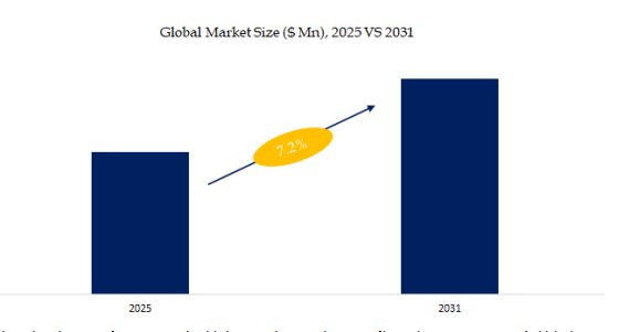
Above data is based on report from QYResearch: Global Semiconductor Grade PEEK Profiles Market Report 2025-2031 (published in 2024). If you need the latest data, plaese contact QYResearch.
Figure. Global Semiconductor Grade PEEK Profiles Top 15 Players Ranking and Market Share (Ranking is based on the revenue of 2024, continually updated)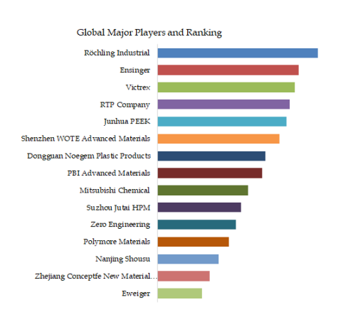
Above data is based on report from QYResearch: Global Semiconductor Grade PEEK Profiles Market Report 2025-2031 (published in 2024). If you need the latest data, plaese contact QYResearch.
Table 1. Semiconductor Grade PEEK Profiles Industry Chain Analysis
Item Description
Upstream Core Chemical Raw Materials Key raw materials for synthesizing PEEK resin, including 4,4'-difluorobenzophenone (DFBP), hydroquinone, diphenyl sulfone, sodium carbonate, etc., among which DFBP is the most critical raw material accounting for a large proportion of the production cost.
Reinforcing and Functional Additives Materials such as carbon fiber, glass fiber, and antistatic agents used to modify the performance of semiconductor-grade PEEK profiles, to meet the requirements of semiconductor manufacturing for corrosion resistance, antistatic properties and mechanical strength.
Production Auxiliary Materials Auxiliary chemicals such as catalysts, end-capping agents involved in the polymerization process of PEEK, which affect the purity and molecular weight distribution of the resin.
Midstream PEEK Resin Synthesis The production of high-purity PEEK resin through polymerization reaction of upstream raw materials, which is the core link with high technical barriers, requiring precise control of impurity content and reaction process.
PEEK Material Modification Carrying out composite modification on PEEK resin according to the performance requirements of semiconductor applications, such as high-purity treatment, anti-static modification, plasma corrosion resistance modification, etc.
Semiconductor Grade PEEK Profiles Processing Processing modified PEEK materials into various profiles through precision molding, CNC machining, injection molding and other processes, including CMP retainer rings, wafer carriers, gas distribution plates, test sockets and other semi-finished or finished components.
Downstream Semiconductor Manufacturing Process Wafer manufacturing (lithography, etching, chemical mechanical polishing), advanced packaging (Chiplet, TSV) and testing links, where semiconductor-grade PEEK profiles are used as key components to ensure process precision and product reliability.
Semiconductor Equipment Manufacturing Manufacturers of semiconductor production and testing equipment integrate PEEK profiles into equipment such as wafer processing machines, testing machines, and deposition equipment as core structural or functional parts.
Semiconductor Related Supporting Fields Emerging semiconductor application scenarios such as semiconductor material testing institutions and semiconductor component maintenance, which have a small but stable demand for semiconductor-grade PEEK profiles for replacement and maintenance of parts.
Source: Secondary Sources, Press Releases, Expert Interviews and QYResearch, 2025
Table 2. Semiconductor Grade PEEK Profiles Industry Development Trends
Development Trends Description
1 Product upgrading for advanced processes Focus on higher purity (lower metal ion content and outgassing), enhanced dimensional accuracy, and specialized functionalization. This includes developing plasma-resistant composite modifications and anti-static surface treatments to adapt to advanced semiconductor manufacturing environments.
2 Process innovation and cost optimization Adopt precision molding and composite modification technologies to improve product uniformity and batch stability. Promote integrated production from raw materials to profiles to reduce processing costs, narrowing the price gap with traditional materials.
3 Deep integration with downstream applications Customize product specifications for key components such as CMP retainer rings, wafer carriers, and test sockets. Collaborate with equipment manufacturers to develop matching profiles for advanced packaging processes like Chiplet and TSV.
Source: Secondary Sources, Press Releases, Expert Interviews and QYResearch, 2025
Table 3. Semiconductor Grade PEEK Profiles Industry Development Opportunities
Development Opportunities Description
1 Surging demand from semiconductor localization The expansion of domestic wafer fabs and the advancement of chip processes drive strong demand for high-performance process materials. Semiconductor grade PEEK profiles, as indispensable components for precision manufacturing, benefit directly from this growth.
2 Policy support for high-end new materials National industrial policies list PEEK as a key development direction, providing R&D subsidies and first-of-its-kind application insurance compensation. These policies accelerate the commercialization of domestic semiconductor grade PEEK products.
3 Replacement of traditional materials With superior heat resistance, chemical corrosion resistance, and mechanical stability, semiconductor grade PEEK profiles are replacing traditional materials like PFA/PTFE in more scenarios, expanding their market share in the semiconductor material sector.
Source: Secondary Sources, Press Releases, Expert Interviews and QYResearch, 2025
Table 4. Semiconductor Grade PEEK Profiles Obstacles/Challenges to Industry Development
Obstacles/Challenges Description
1 High technical and process barriers Strict requirements for impurity control (metal ions ≤1ppm) and precision processing pose significant challenges. Core technologies such as high-purity polymerization and composite modification are still dominated by international enterprises.
2 Dependence on upstream raw materials and equipment High-purity raw materials like DFBP have insufficient domestic supply, relying heavily on imports. High-end production equipment such as precision injection molding machines and CNC processing tools also face import restrictions.
3 Long customer certification cycles and high thresholds Downstream semiconductor manufacturers have strict supplier audits, with product verification cycles lasting 1–3 years. New entrants struggle to gain market access due to the need for long-term reliability testing and technical validation.
Source: Secondary Sources, Press Releases, Expert Interviews and QYResearch, 2025
Looking ahead, the market will maintain robust growth momentum, with trends focusing on three core directions: first, product upgrading toward higher purity, better dimensional accuracy, and specialized functionalization (such as enhanced corrosion resistance for plasma environments and optimized dielectric properties for high-frequency applications) to adapt to advanced semiconductor processes; second, deeper integration of the industrial chain, as manufacturers strengthen independent R&D of raw materials and precision processing technologies to reduce supply chain risks and cost pressure; third, expanded application scenarios driven by technological innovations like 2.5D/3D advanced packaging and green manufacturing, coupled with policy support for domestic semiconductor materials, which will further promote the widespread adoption of semiconductor grade PEEK profiles and solidify their role in the high-end semiconductor supply chain.
About QYResearch
QYResearch founded in California, USA in 2007.It is a leading global market research and consulting company. With over 17 years’ experience and professional research team in various cities over the world QY Research focuses on management consulting, database and seminar services, IPO consulting, industry chain research and customized research to help our clients in providing non-linear revenue model and make them successful. We are globally recognized for our expansive portfolio of services, good corporate citizenship, and our strong commitment to sustainability. Up to now, we have cooperated with more than 60,000 clients across five continents. Let’s work closely with you and build a bold and better future.
QYResearch is a world-renowned large-scale consulting company. The industry covers various high-tech industry chain market segments, spanning the semiconductor industry chain (semiconductor equipment and parts, semiconductor materials, ICs, Foundry, packaging and testing, discrete devices, sensors, optoelectronic devices), photovoltaic industry chain (equipment, cells, modules, auxiliary material brackets, inverters, power station terminals), new energy automobile industry chain (batteries and materials, auto parts, batteries, motors, electronic control, automotive semiconductors, etc.), communication industry chain (communication system equipment, terminal equipment, electronic components, RF front-end, optical modules, 4G/5G/6G, broadband, IoT, digital economy, AI), advanced materials industry Chain (metal materials, polymer materials, ceramic materials, nano materials, etc.), machinery manufacturing industry chain (CNC machine tools, construction machinery, electrical machinery, 3C automation, industrial robots, lasers, industrial control, drones), food, beverages and pharmaceuticals, medical equipment, agriculture, etc.

Global Semiconductor Grade PEEK Profiles Market Outlook, In‑Depth Analysis & Forecast to 2032

Published Date: 2026-03-24

Pages: 155

Report ld: 6273088
Price:USD 4900.00
(Single User License)
Global Semiconductor Grade PEEK Profiles Sales Market Report, Competitive Analysis and Regional Opportunities 2026-2032
Published Date: 2026-03-24
Pages: 95
Report ld: 6267541
Price:USD 4250.00
(Single User License)
Semiconductor Grade PEEK Profiles- Global Market Share and Ranking, Overall Sales and Demand Forecast 2026-2032
Published Date: 2026-01-19
Pages: 115
Report ld: 5775706
Price:USD 3950.00
(Single User License)
Global Semiconductor Grade PEEK Profiles Market Research Report 2026
Published Date: 2026-01-08
Pages: 136
Report ld: 5584698
Price:USD 2900.00
(Single User License)
Global Semiconductor Grade PEEK Profiles Market Outlook, In‑Depth Analysis & Forecast to 2031
Published Date: 2025-11-27
Pages: 170
Report ld: 4812373
Price:USD 4900.00
(Single User License)
Global Semiconductor Grade PEEK Profiles Sales Market Report, Competitive Analysis and Regional Opportunities 2025-2031
Published Date: 2025-11-27
Pages: 91
Report ld: 4525455
Price:USD 4250.00
(Single User License)


Competition
Key players, new entrants,acquisitions, mergers and expansions,development trends and challenges.

Industry Analysis
Rawmaterial, application, product type, demand,supply,downstream, supply chain etc.

Market Size
Capacity, production, sales, revenue, price, cost etc.

Customized Information
We can offer customized survey and information to meet ourclient's need.
