Semiconductor Metrology and Inspection Market Set to Hit 21090 Million USD by 2026 – What Industry Leaders Are Doing Differently


Product Overview and Scope of Semiconductor Metrology and Inspection
Semiconductor metrology and inspection are crucial manufacturing processes that use advanced measurement and testing to ensure the quality, performance, and yield of semiconductor devices. Metrology uses scientific measurement to characterize materials and structures like film thickness and line width, while inspection identifies defects such as particles, voids, and misalignment. Together, they are vital for process control, troubleshooting, and validating the precision of complex 3D designs in modern chip fabrication.
Figure. Semiconductor Metrology and Inspection Picture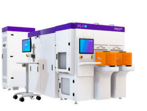
Secondary Sources and QYResearch, 2025
Upstream: High Concentration of Core Components
Optics: Deep ultraviolet/extreme ultraviolet light sources, ultra-precision objectives, interferometers, spectrometers—US, Japanese, and German companies hold over 90% market share;
Electron beam: Field emission guns, high-voltage power supplies, electromagnetic lenses, electron detectors—monopolized by Hitachi (Japan), KLA (USA), etc.;
High-speed motion stages: Air-floating/magnetic levitation platforms, nanoscale laser rulers, reliant on imports;
Software/algorithms: Scattering instrument modeling, OCD libraries, AI defect classification, and EDA+optical co-simulation are still controlled by Synopsys and KLA.
As a result, 60%–70% of the cost in the BOM of domestically produced equipment comes from imported key components, making it one of the semiconductor equipment segments with the lowest domestic production rate.
Midstream: Complete Machine Manufacturing and System Integration Globally, a "one-superpower-four-strong" pattern emerges—KLA holds a 54% market share, while Applied Materials, Hitachi High-Tech, ASML (Litho+EBI), and Lasertec together account for 35%. Chinese domestic manufacturers (such as Zhongke Feice, Jingce Electronics, Xinkailai, and Chuangrui Spectrum, etc.) still hold a combined market share of less than 8%, mostly achieving breakthroughs at 28 nm and above nodes, entering second-tier wafer fabs through an "equipment + algorithm services + leasing" model.
Downstream: Wafer Manufacturing, Advanced Packaging, Third-Party Laboratories
Front-end wafer fabs (logic 3/5/7 nm, 3D NAND, DRAM) account for 79% of equipment shipments, requiring detection sensitivity <20 nm and measurement accuracy <0.1 nm;
Advanced packaging (TSV, HBM, 2.5D) requires large-size warp, bump height, and RDL defect detection, bringing a 45% increase to the SiC and HBM testing market in 2025;
Third-party testing laboratories (such as Sembcorp Nanotech) provide failure analysis and process diagnostics, with revenue increasing by 29% year-on-year in the first half of 2025, becoming a new growth point for the specialization of the industry chain.
Semiconductor Metrology and Inspection Market Summary
According to the new market research report “Global Semiconductor Metrology and Inspection Market Report 2024-2030”, published by QYResearch, the global Semiconductor Metrology and Inspection market size is projected to reach USD 35.51 billion by 2030, at a CAGR of 10.8% during the forecast period.
Figure. Global Semiconductor Metrology and Inspection Market Size (US$ Million), 2020-2031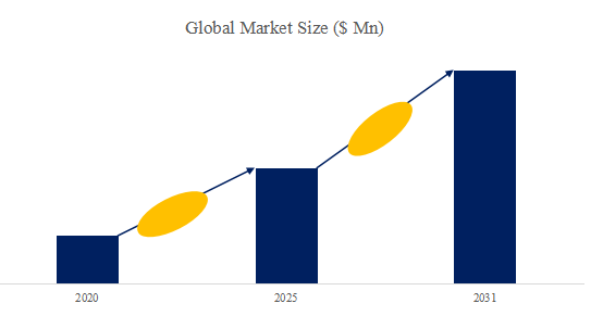
Above data is based on report from QYResearch: Global Semiconductor Metrology and Inspection Market Report 2025-2031 (published in 2025). If you need the latest data, plaese contact QYResearch.
Figure. Global Semiconductor Metrology and Inspection Top 15 Players Ranking and Market Share (Ranking is based on the revenue of 2024, continually updated)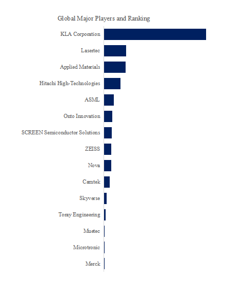
Above data is based on report from QYResearch: Global Semiconductor Metrology and Inspection Market Report 2025-2031 (published in 2025). If you need the latest data, plaese contact QYResearch.
According to QYResearch Top Players Research Center, the global key manufacturers of Semiconductor Metrology and Inspection include KLA Corporation, Lasertec, Applied Materials, Hitachi High-Technologies, ASML, Onto Innovation, SCREEN Semiconductor Solutions, ZEISS, Nova, Camtek, etc. In 2023, the global top five players had a share approximately 75.0% in terms of revenue.
Figure. Semiconductor Metrology and Inspection, Global Market Size, Split by Product Segment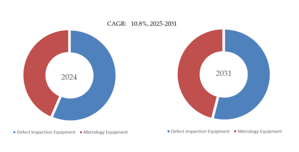
Based on or includes research from QYResearch: Global Semiconductor Metrology and Inspection Market Report 2025-2031.
In terms of product type, currently Defect Inspection Equipment is the largest segment, hold a share of 56.4%.
Figure. Semiconductor Metrology and Inspection, Global Market Size, Split by Application Segment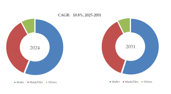
Based on or includes research from QYResearch: Global Semiconductor Metrology and Inspection Market Report 2025-2031.
In terms of product application, currently Wafer is the largest segment, hold a share of 56.1%.
About QYResearch
QYResearch founded in California, USA in 2007.It is a leading global market research and consulting company. With over 17 years’ experience and professional research team in various cities over the world QY Research focuses on management consulting, database and seminar services, IPO consulting, industry chain research and customized research to help our clients in providing non-linear revenue model and make them successful. We are globally recognized for our expansive portfolio of services, good corporate citizenship, and our strong commitment to sustainability. Up to now, we have cooperated with more than 60,000 clients across five continents. Let’s work closely with you and build a bold and better future.
QYResearch is a world-renowned large-scale consulting company. The industry covers various high-tech industry chain market segments, spanning the semiconductor industry chain (semiconductor equipment and parts, semiconductor materials, ICs, Foundry, packaging and testing, discrete devices, sensors, optoelectronic devices), photovoltaic industry chain (equipment, cells, modules, auxiliary material brackets, inverters, power station terminals), new energy automobile industry chain (batteries and materials, auto parts, batteries, motors, electronic control, automotive semiconductors, etc.), communication industry chain (communication system equipment, terminal equipment, electronic components, RF front-end, optical modules, 4G/5G/6G, broadband, IoT, digital economy, AI), advanced materials industry Chain (metal materials, polymer materials, ceramic materials, nano materials, etc.), machinery manufacturing industry chain (CNC machine tools, construction machinery, electrical machinery, 3C automation, industrial robots, lasers, industrial control, drones), food, beverages and pharmaceuticals, medical equipment, agriculture, etc.

Global Semiconductor Metrology and Inspection Sales Market Report, Competitive Analysis and Regional Opportunities 2026-2032

Published Date: 2026-01-05

Pages: 101

Report ld: 5575813
Price:USD 4250.00
(Single User License)
Global Semiconductor Metrology and Inspection Market Research Report 2026
Published Date: 2026-01-05
Pages: 146
Report ld: 5573500
Price:USD 2900.00
(Single User License)
Semiconductor Metrology and Inspection- Global Market Share and Ranking, Overall Sales and Demand Forecast 2026-2032
Published Date: 2026-01-05
Pages: 141
Report ld: 5511450
Price:USD 3950.00
(Single User License)
Semiconductor Metrology and Inspection - Global Market Share and Ranking, Overall Sales and Demand Forecast 2025-2031
Published Date: 2025-12-05
Pages: 139
Report ld: 5536337
Price:USD 3950.00
(Single User License)
Global Semiconductor Metrology and Inspection Sales Market Report, Competitive Analysis and Regional Opportunities 2025-2031
Published Date: 2025-12-05
Pages: 104
Report ld: 4929787
Price:USD 4250.00
(Single User License)
Global Semiconductor Metrology and Inspection Market Outlook, In‑Depth Analysis & Forecast to 2031
Published Date: 2025-12-05
Pages: 177
Report ld: 4806703
Price:USD 4900.00
(Single User License)


Competition
Key players, new entrants,acquisitions, mergers and expansions,development trends and challenges.

Industry Analysis
Rawmaterial, application, product type, demand,supply,downstream, supply chain etc.

Market Size
Capacity, production, sales, revenue, price, cost etc.

Customized Information
We can offer customized survey and information to meet ourclient's need.
