Semiconductor Photoresist Market Set to Hit 3522 Million USD by 2026 – What Industry Leaders Are Doing Differently


Semiconductor Photoresists Market Summary
Photoresist (PR) is a chemical essential for semiconductor manufacturing. The photoresists known as a photosensitive material, initiate a chemical reaction in the light. It is a chemical that plays an essential role in photolithography, a technology that is involved in the manufacture of semiconductor devices. In the semiconductor manufacturing, the exposure process that a photoengraving technique is applied to reduce and transfer the design drawn on the original plate (photomask) onto the silicon chip. To create power-saving, high-performance semiconductors, the circuits that are to be transferred need to be rendered smaller.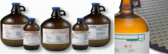
According to the new market research report “Global Semiconductor Photoresists Market Report 2025-2031”, published by QYResearch, the global Semiconductor Photoresists market size is projected to reach USD 5.1 billion by 2032, at a CAGR of 6.4% during the forecast period.
Figure. Global Semiconductor Photoresists Market Size (US$ Million), 2020-2031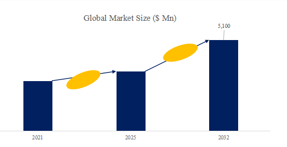
Above data is based on report from QYResearch Semiconductor Research Center: Global Semiconductor Photoresists Market Report 2025-2031 (published in 2025). If you need the latest data, plaese contact QYResearch.
Figure. Global Semiconductor Photoresists Market Size (US$ Million), by Type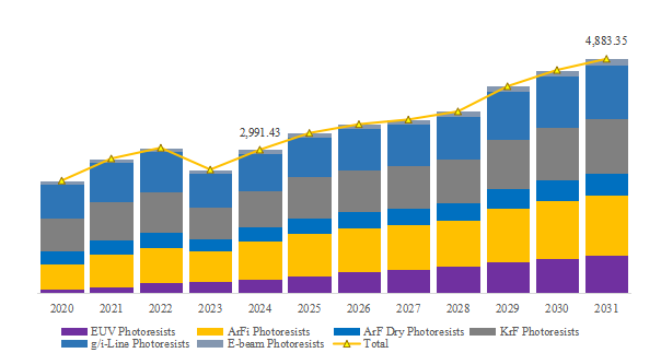
Above data is based on report from QYResearch Semiconductor Research Center: Global Semiconductor Photoresists Market Report 2025-2031 (published in 2025). If you need the latest data, plaese contact QYResearch.
Structurally, the mix in 2025 is still DUV-dominated: ArFi (~26.1%) + KrF (~25.5%) + g/i-Line (~24.6%) ≈ 76% of total value, reflecting the reality that even in leading-edge flows, EUV is used for the most intricate layers while many remaining layers continue to be patterned with DUV, and both platforms run in parallel for years. Within DUV, ArFi’s weight is also consistent with technology boundaries: for many “mainstream-to-advanced mature” nodes, immersion ArF remains a foundational lithography capability. Meanwhile, EUV photoresists are the clear growth engine (rising from ~$80M to ~$374M from 2020 to 2025; fastest growth rate among your segments), but still only ~11.2% of the 2025 total—i.e., EUV is driving the growth, while DUV still carries the volume and breadth of layers.
Looking forward over the next few years, the direction is: EUV grows fastest; ArFi stays resilient; KrF and g/i-Line remain stable-to-slight growth; ArF Dry grows modestly; E-beam grows steadily but niche—each for different “real-fab” reasons. EUV resists should keep outgrowing the market because EUV layer counts and EUV exposure intensity rise with continued scaling, and the ecosystem is now also entering the High-NA EUV era (tool milestones such as acceptance testing and High-NA platform ramp are now public), which tightens resist requirements and pulls more innovation spend into EUV materials (stochastics/roughness/sensitivity tradeoffs, outgassing control, etc.). ArFi resists are likely to remain the “workhorse premium DUV” category: even where EUV expands, ArFi continues to print many non-EUV layers and supports huge installed bases at 28/22/16/14nm-class and below, and a lot of capacity being added globally is still in ranges that rely on ArFi capability. ArF Dry typically tracks a broad swath of mature logic and specialty IC production, so expect low-to-mid single-digit growth driven more by wafer-start expansion and mix (specialty, analog, PMIC, CIS, etc.) than by “node shrinks.” KrF should stay solid because it sits in the cost/performance sweet spot for many mature nodes and selected tighter-pattern layers where ArF isn’t required; its main driver is mature-node capacity + automotive/industrial stability, with cyclicality tied to overall wafer starts. g/i-Line is “sticky” for thick resist and back-end / packaging-centric lithography, so advanced packaging scaling (more RDL layers, bumping/plating processes, wafer-/panel-level packaging) tends to underpin demand even when leading-edge front-end is soft; suppliers explicitly position g/i-line portfolios around thick-film variants and packaging-related patterning use-cases (including RDL). E-beam resists should grow steadily (but remain small) because advanced mask making—especially EUV masks—depends heavily on e-beam lithography resist performance, and mask complexity rises as design rules tighten. Macro-wise, a supportive tailwind for all categories is the expectation that wafer-fab investment and capacity expansion are lifted by AI-driven logic and memory demand into 2026–2027, which typically flows through into lithography materials consumption with a lag.
According to QYResearch, the global key manufacturers of Semiconductor Photoresists include TOK, Shin-Etsu Chemical, JSR, Qnity, Sumitomo Chemical, etc. in 2025, the global top five players had a share approximately 79.0% in terms of revenue.
About QYResearch
QYResearch founded in California, USA in 2007. It is a leading global market research and consulting company. With over 17 years’ experience and professional research team in various cities over the world QY Research focuses on management consulting, database and seminar services, IPO consulting, industry chain research and customized research to help our clients in providing non-linear revenue model and make them successful. We are globally recognized for our expansive portfolio of services, good corporate citizenship, and our strong commitment to sustainability. Up to now, we have cooperated with more than 60,000 clients across five continents. Let’s work closely with you and build a bold and better future.
QYResearch is a world-renowned large-scale consulting company. The industry covers various high-tech industry chain market segments, spanning the semiconductor industry chain (semiconductor equipment and parts, semiconductor materials, ICs, Foundry, packaging and testing, discrete devices, sensors, optoelectronic devices), photovoltaic industry chain (equipment, cells, modules, auxiliary material brackets, inverters, power station terminals), new energy automobile industry chain (batteries and materials, auto parts, batteries, motors, electronic control, automotive semiconductors, etc.), communication industry chain (communication system equipment, terminal equipment, electronic components, RF front-end, optical modules, 4G/5G/6G, broadband, IoT, digital economy, AI), advanced materials industry Chain (metal materials, polymer materials, ceramic materials, nano materials, etc.), machinery manufacturing industry chain (CNC machine tools, construction machinery, electrical machinery, 3C automation, industrial robots, lasers, industrial control, drones), food, beverages and pharmaceuticals, medical equipment, agriculture, etc.

Global Semiconductor Photoresist Market Outlook, In‑Depth Analysis & Forecast to 2032

Published Date: 2026-01-23

Pages: 212

Report ld: 5785278
Price:USD 4900.00
(Single User License)
Global Semiconductor Photoresist Sales Market Report, Competitive Analysis and Regional Opportunities 2026-2032
Published Date: 2026-01-23
Pages: 125
Report ld: 5572716
Price:USD 4250.00
(Single User License)
Global Semiconductor Photoresist Market Research Report 2026
Published Date: 2026-01-23
Pages: 166
Report ld: 5525782
Price:USD 2900.00
(Single User License)
Semiconductor Photoresist- Global Market Share and Ranking, Overall Sales and Demand Forecast 2026-2032
Published Date: 2026-01-23
Pages: 180
Report ld: 5507819
Price:USD 3950.00
(Single User License)
Global Semiconductor Photoresist Sales Market Report, Competitive Analysis and Regional Opportunities 2025-2031
Published Date: 2025-09-10
Pages: 126
Report ld: 4846840
Price:USD 4250.00
(Single User License)
Global Semiconductor Photoresist Market Outlook, In‑Depth Analysis & Forecast to 2031
Published Date: 2025-08-08
Pages: 212
Report ld: 4921528
Price:USD 4900.00
(Single User License)


Competition
Key players, new entrants,acquisitions, mergers and expansions,development trends and challenges.

Industry Analysis
Rawmaterial, application, product type, demand,supply,downstream, supply chain etc.

Market Size
Capacity, production, sales, revenue, price, cost etc.

Customized Information
We can offer customized survey and information to meet ourclient's need.
